Design Combinational Circuit Three Inputs

Three Input Circuit With Redundant Gates Simple Circuit Algebra Equations Some Text
Q 4 4 Design A Combinational Circuit With Three Inputs And One Output A The Output Is 1 When Youtube
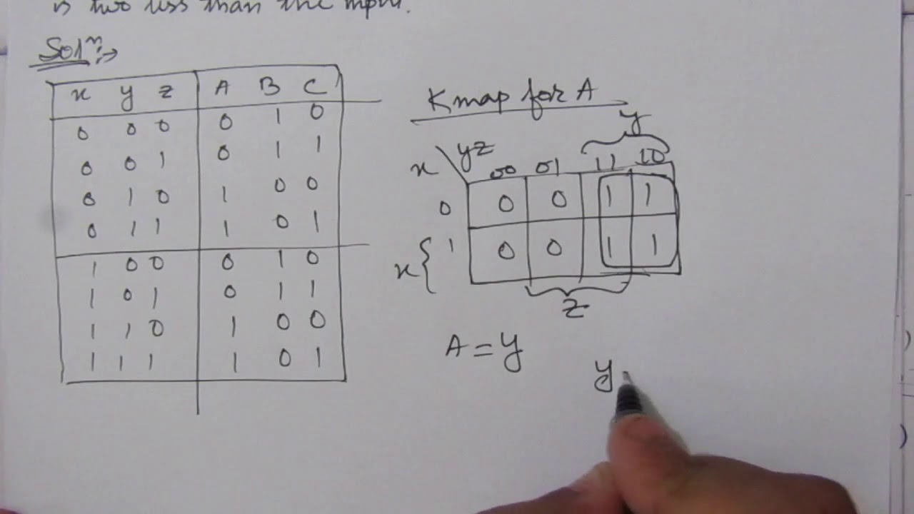
Q 4 5 Design A Combinational Circuit With Three Inputs X Y And Z And Three Outputs A B And C Youtube

Pin On Digital Logic Circuits

Combinational Logic Circuits Functions And Classification Circuit Electronics Projects Logic
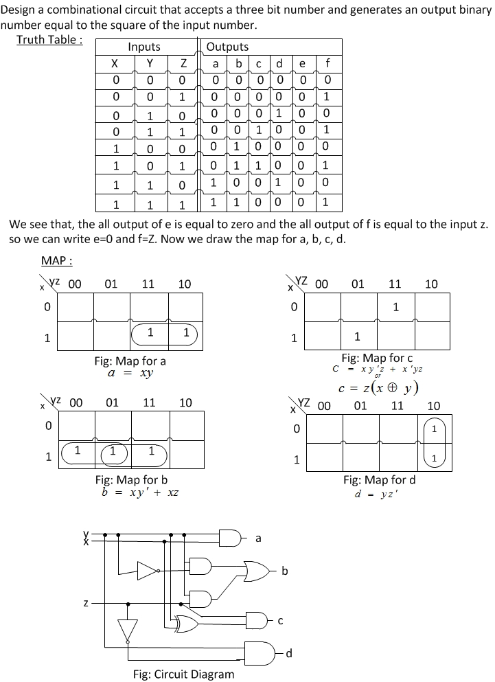
Logic Circuit Of Square Of 3 Input Variable Sukanta S Diary

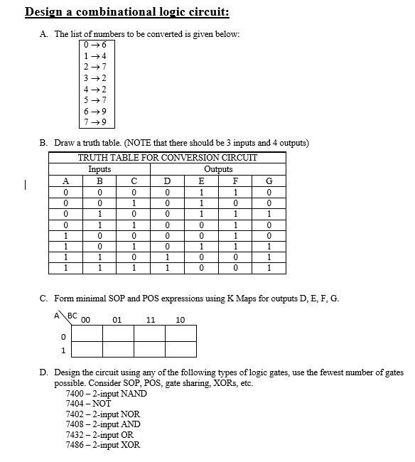
Construct the truth table to define relationship between inputs and outputs.
Design combinational circuit three inputs. And z should be true if the number is a. When the binary input is 0 1 2 or 3 the binary output is one greater than the input. Half adder is a combinational logic circuit with two inputs and two outputs. When the binary input is 0 1 2 or 3 the binary out.
When the binary input is 4 5 6 or 7 the binary output is one less than the input. The design procedure for combinational logic circuits starts with the problem specification and comprises the following steps. Show transcribed image text. Design a combinational circuit that adds 3 to the inputs in 2 bit data.
Design a combinational circuit with 4 inputs a3 a2 a1 a0. We re going to elaborate few important combinational circuits as follows. When the binary input is 0 1 2 or 3 the binary output is 1 greater than the input. 4 5 design a combinational circuit with three inputs x y and z and three outputs a b and c.
Determine required number of inputs and outputs from the specifications. A combinational circuit can have an n number of inputs and m number of outputs. This problem has been solved. Get more help from.
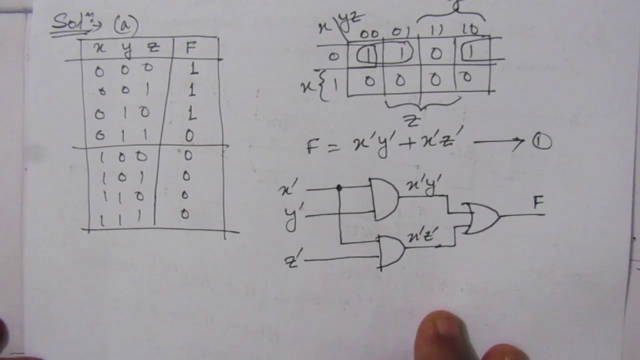
The logic diagram is drawn. Design a combinational circuit with three inputs and one output. And three outputs x y z. Design a combinational circuit with three inputs x y and z and three outputs a b and c.
When the binary input is 4 5 6 or 7 the binary output is one less than the input. When the binary input is 0 1 2 or 3 the binary output is one greater than the input. A the output is 1 when the binary value of the inputs is less than3. Design a combinational circuit with three inputs x y z and three outputs a b and c.
When the binary input is 4 5 6 or 7 the binary output is one less than the input. The simplified boolean function for each output is obtained using k map tabulation method and boolean algebra rules. Design a combinational circuit that adds 3 to the inputs in 2 bit data. Design a combinational circuit with three inputs x y and z and the three outputs a b and c.
To design a combinational logic circuit use the following procedures. Derive the truth table for each of the outputs based on their relationships to the input. The half adder circuit is designed to add two single bit binary number a and b. The inputs represent a binary number in the range 0 15 and the outputs represent characteristics of the numbers.

Design Of Parallel Adder In 2020 Binary Number Parallel Simple Solutions
Https Ece Uwaterloo Ca Msachdev Ece223 Assignment4 Solution 3rd Edition Pdf

1 Bit Comparator Logic Electronics Circuit Bits

2 Bit Synchronous Up Counter Electronics Circuit Circuit Digital
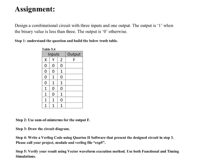
Solved Assignment Design A Combinational Circuit With Th Chegg Com
Combinational Circuits Circuit Electronics Circuit Block Diagram

Combinational Logic Circuits 3 Logic What Is Meant Circuit
Solved Design A Combinational Logic Circuit The List Of Chegg Com

3 Bit Synchronous Up Down Counter Electronics Circuit Counter Circuit

Logic And Gate Tutorial Truth Table Electronics Area Logic Tutorial Truth

Pin On Electrical

Pin On Mrmgate

Combinational Circuit Using Logic Gates Digital Electronics Electronics Area Circuit Logic Electronics

Combinational Logic Logic Electronic Engineering Circuit

Binary To Gray Code Converter 3 Bit Coding Converter Binary

Multiplexers Using Logic Gates Circuit Design Electronics Circuit Circuit

4 Bit Parallel Subtractor Parallel Logic Design

4 Bit Comparator Logic Electronics Circuit Bits
Https Encrypted Tbn0 Gstatic Com Images Q Tbn 3aand9gctwfpfbf0ekbpk63pq8e9jykh7z6h5ez0q Radxdse88hiwcusz Usqp Cau

Gray To Binary Code Converter 4 Bit Coding Binary Converter

Logic Gates Symbols Electronic Engineering Electronics Basics Electricity

3 Best Transformerless Inverter Circuits Homemade Circuit Projects Electronic Circuit Projects Circuit Projects Circuit Design

Digital Logic Gates Using Nand Gates Electronics Electrical Circuit Design Digital Electronics

Simulation Of A Half Adder Circuit With 4 Basic Gates Using Tina Circuit Design Simulation Circuit Simulator

Cryptographic Coprocessor Design In Vhdl Combinational Logic Unit And Register File Are Two Major Components Of The Coprocessor Design Logic Projects
Qimm7owvj5tl M

Tl084 Circuits Jfet Input Op Amp Datasheet Eleccircuit Com In 2020 Basic Electronic Circuits Electronics Circuit Electronic Circuit Projects

Circuit Daigram Of Automatic Gain Control With Amlifier In 2020 Circuit Design Circuit Common Emitter

Binary To Excess 3 Code Converter 3 Bit Coding Binary Converter

High Voltage Dc Generator Circuit 12vdc Input 10 000vdc Output Electrical Enginee Electronic Circuit Projects Electronic Engineering Electronics Circuit

Pin On Electronics

Pin Em Electronic Schematics

4 Bit Asynchronous Up Down Counter Counter Electronics Circuit Circuit

6n137 Application Circuit Circuit High Speed Nand Gate


Unijunction Transistor Ujt Equivalent Model Circuit Electronics Area Transistors Circuit Electronics Components

Pin On Electronic Schematics

Full Adder Using Multiplexers Electronics Circuit Circuit Design Circuit

Difference Between Combinational And Sequential Circuit Sequential Logic Circuit

Decade Counter Electronics Circuit Counter Circuit

Logic Gate Control Systems 2 Output Device Logic Circuit

Power Supply For Audio Amplifier Circuit Multiple Output 12v 15v 35v Audio Amplifier Power Supply Circuit Basic Electronic Circuits

