Design A Combinational Circuit That Generates Output As 1 Only For Particular Input Pattern
Q 4 4 Design A Combinational Circuit With Three Inputs And One Output A The Output Is 1 When Youtube
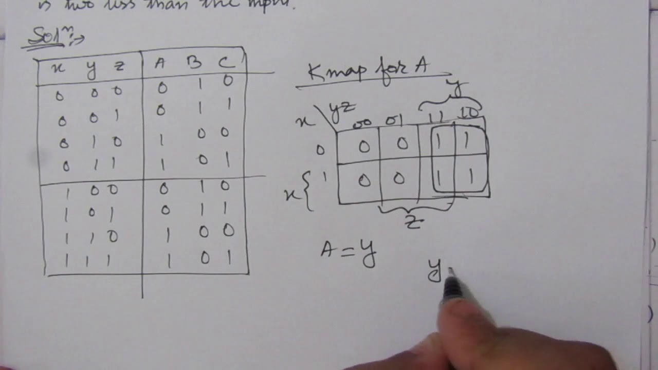
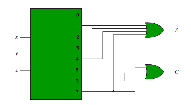
Q 4 5 Design A Combinational Circuit With Three Inputs X Y And Z And Three Outputs A B And C Youtube
Https Ece Uwaterloo Ca Msachdev Ece223 Assignment4 Solution 3rd Edition Pdf
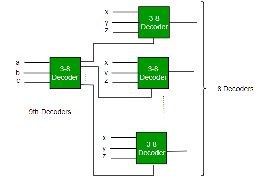
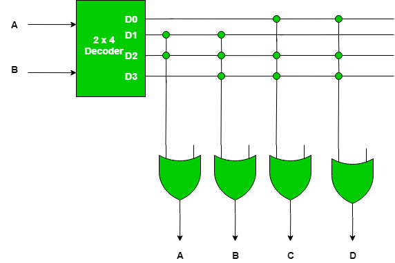
Combinational Circuits Using Decoder Geeksforgeeks

4 1 Annotated Slides 4 Combinational Logic Computation Structures Electrical Engineering And Computer Science Mit Opencourseware

Priority Encoder And Digital Encoder Tutorial
This additional or extra bit is termed as a parity bit.
Design a combinational circuit that generates output as 1 only for particular input pattern. In even parity bit scheme the parity bit is 0 if there are even number of 1s in the data stream and the parity bit is 1 if there. Sequential circuits are those which are dependent on clock cycles and depends on present as well as past inputs to generate any output. Compare two 1 bit numbers. As we saw in part 1 their output is a very simple function of their inputs describable with a very simple truth table.
Terms the each output is a function of the inputs. Design a circuit that has a 3 bit binary input and a single output that output 1 if it is a prime number. A decoder can be thought of as converting an n bit input to a 2 n output. For n input variables there are 2n possible combinations of binary input values.
This is time independent. A multiplexer is often written as mux in the abbreviated form. The control unit must select the correct two registers based on these two 4 bit patterns in the instruction. Draw the logic diagram using the and or gates and discuss its inference.
For each possible input combination there is one and only one possible output combination a combinational circuit can be describe by m boolean functions one. Combinational circuit in this output depends only upon present input. It is designed easy. The previous state of input does not have any effect on the present state of the circuit.
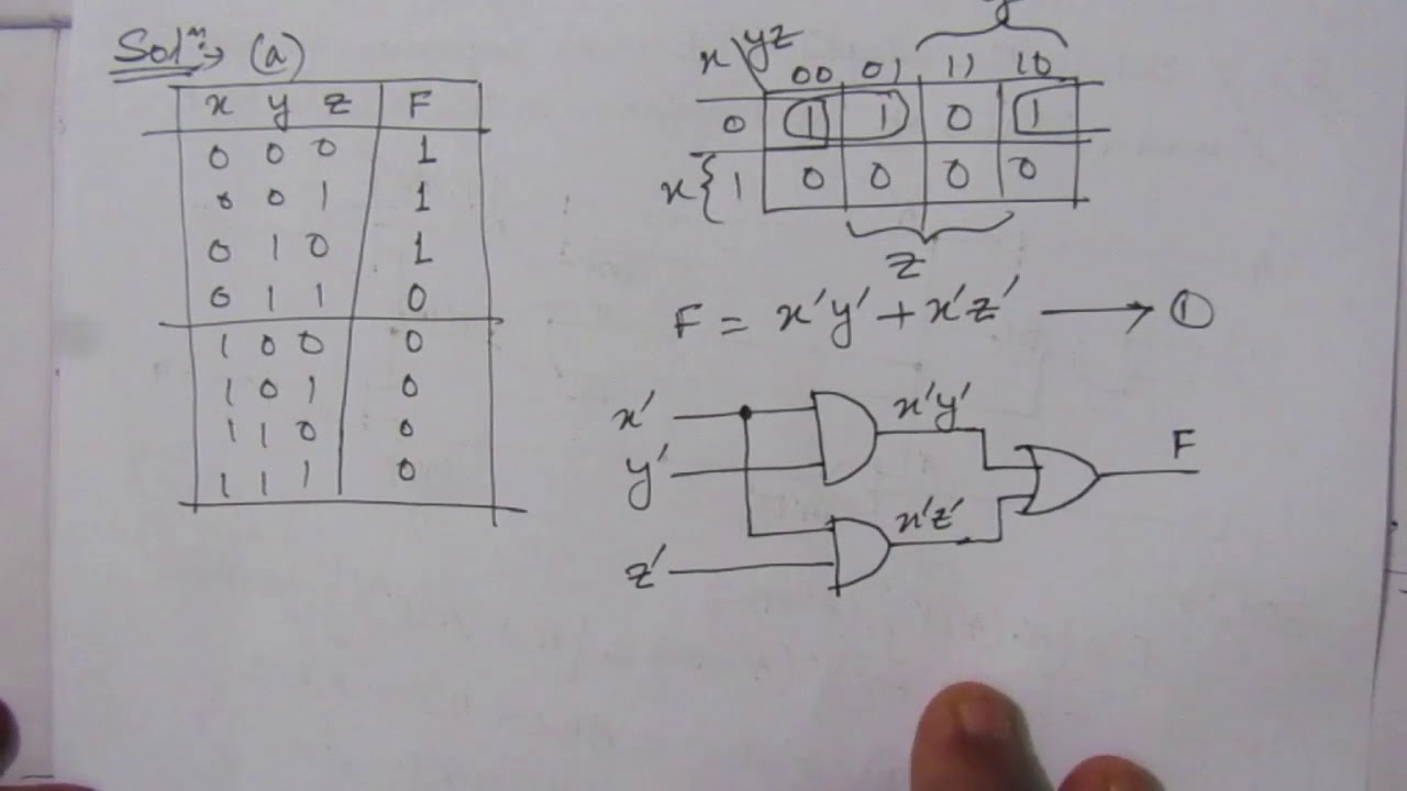
Multiplexer is a combinational logic circuit which allows only one input at a particular time to generate the output. It is combinational circuit that accepts an n 1 bit stream data and generates the additional bit that is to be transmitted with the bit stream. The signals which control which input will be reflected at the output end is determined by the select input lines. Questions marks 1 4m design a combinational circuit that generates output as 1 only for particular input pattern student s vtu number use k map for boolean minimization.
A device with n binary inputs and 2 n binary outputs. The combinational circuit do not use any memory. It uses a decoder circuit to perform this selection. A combinational circuit can have an n number of inputs and m number of outputs.
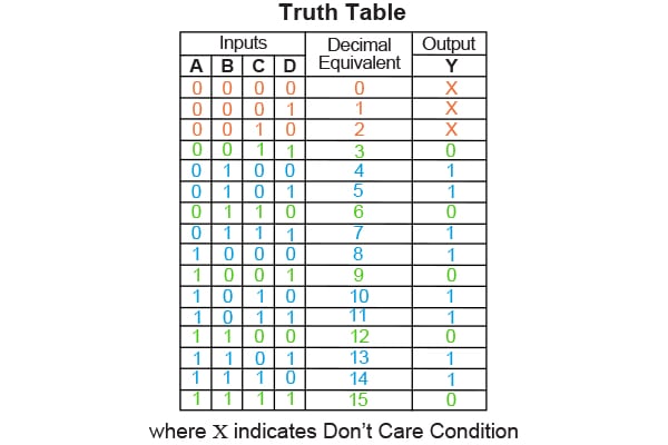
Repeated numbers should consider as single number design a combinational circuit that generates. Draw the truth table for a combinational circuit that generates output as 1 only for particular input pattern double the student s vtu number 14974 write the boolean expression in standard sop form design nand nand implementation nor nor implementation for that expression derived from i design a data selector circuit for that truth. Eg 2 10 3 10 5 10 7 10. The output of combinational circuit at any instant of time depends only on the levels present at input terminals.
A combinational circuit consists of input variables n logic gates and output variables m. These functions can be described using logic expressions but is most often at least initially using truth tables. Each bit pattern at the input causes exactly one of the 2 n to equal 1.
Https Ece Uwaterloo Ca Cgebotys New Quizzes Extratutorialans Pdf

Combinational Logic Circuits Using Logic Gates
Http Web4 Uwindsor Ca Users A Alginahi 60 265 Nsf 831fc2c71873e46285256d6e006c367a 9391445fba4fc83f85256fc8004827a3 File Assignment3 Solutions 20265 Pdf

Tn528i6rzbsbkm

Sequential Logic Circuits Circuit Digital Circuit Logic
Http Www Ee Ic Ac Uk Pcheung Teaching De1 Ee Lectures Lecture 2011 20 20logic 20gates 20and 20boolean 20 X2 Pdf
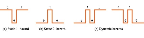
Hazards In Combinational Logic Technical Articles
5 Logic Circuits

Signal Processing Fundamentals Signal Processing Compressor Fundamental
Classification And Programming Of Read Only Memory Rom Geeksforgeeks

Combinational Circuit An Overview Sciencedirect Topics

Moore Machine An Overview Sciencedirect Topics

Conversion Of Flip Flops From One Flip Flop To Another

Ask Modulator Circuit Diagram Circuit Diagram Modulators Circuit
Design 101 Sequence Detector Mealy Machine Geeksforgeeks

Sequential Circuits An Overview Sciencedirect Topics

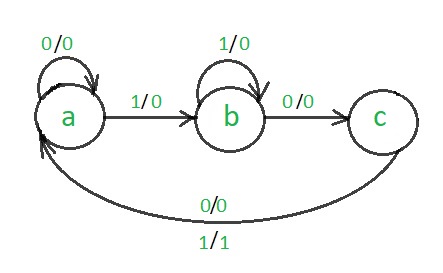
State Diagrams And State Tables

7 Finite State Machine Fpga Designs With Verilog And Systemverilog Documentation
Https Encrypted Tbn0 Gstatic Com Images Q Tbn 3aand9gcszd58ubycdw G3exhx8g9ezn9pqne01jz7kuwquuxzodjbsk7u Usqp Cau

Synchronous Sequential Circuit An Overview Sciencedirect Topics

Logic Circuits An Overview Sciencedirect Topics

Rectification Of A Three Phase Supply Using Diodes
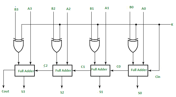
4 Bit Binary Adder Subtractor Geeksforgeeks
Vlsi Design Quick Guide Tutorialspoint

Pin On Energia
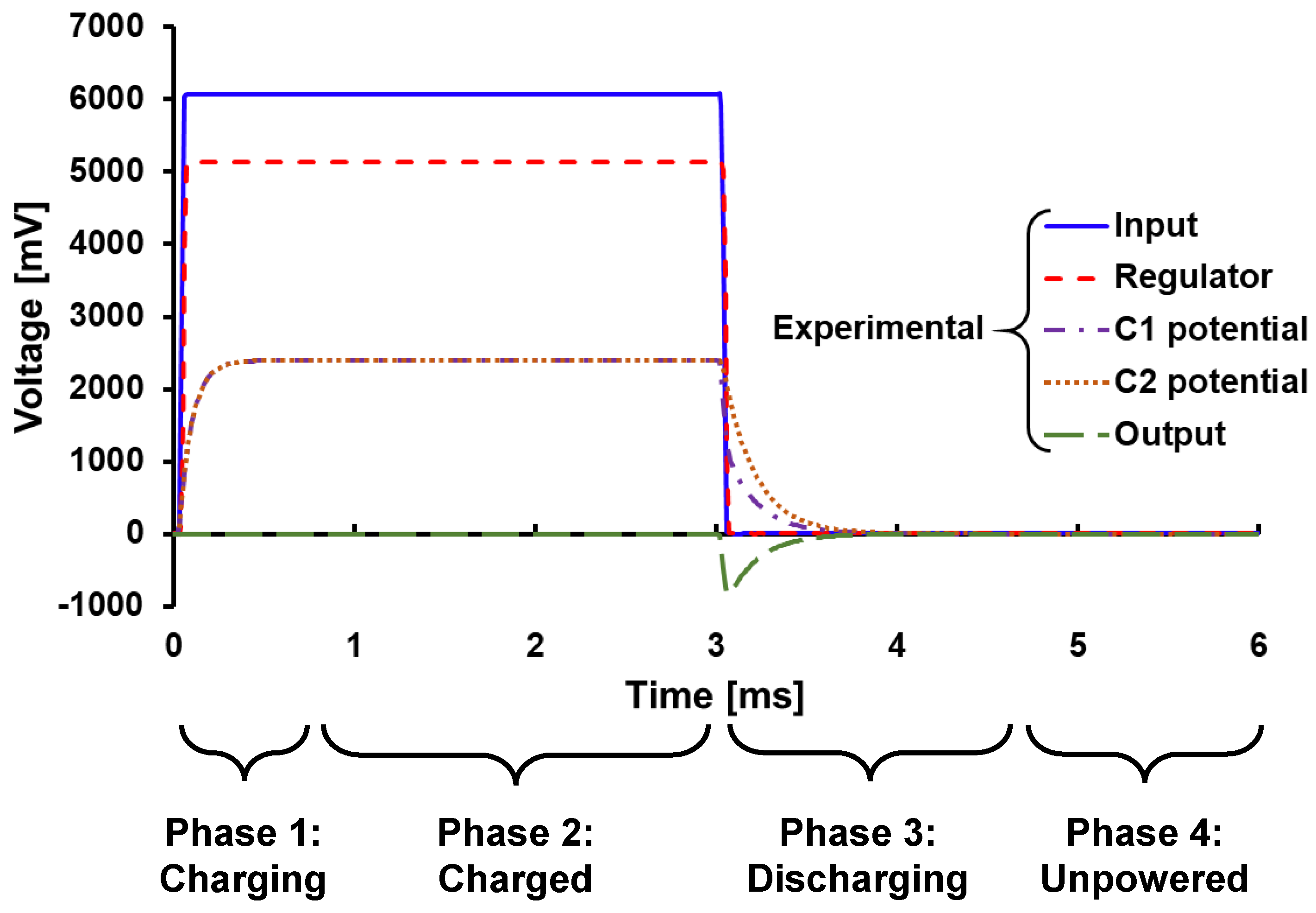
Electronics Free Full Text A Pulse Generation Circuit For Studying Waveform Effects On Neurostimulation Html

Sequential Circuit An Overview Sciencedirect Topics

Sequential Logic An Overview Sciencedirect Topics

Block Diagram Of 8051 Microcontroller Based Wireless Notice Board Microcontrollers Pic Microcontroller Block Diagram

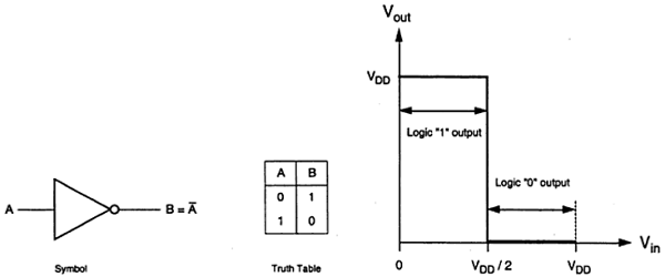
Logic Not Function Digital Logic Gates

Programmable Peripheral Interface 8255 Geeksforgeeks

Basic Logic Gates Worksheet Digital Circuits

Service Manuals Service Schematics Datasheets Smd Code Coding Electronic Circuit Design Electronics Circuit

Logic Nand Gate Tutorial With Nand Gate Truth Table
The Karnaugh Map Boolean Algebraic Simplification Technique Technical Articles
Http Resource Download Wjec Co Uk S3 Amazonaws Com Vtc 2016 17 16 17 1 9 Gce Electronics Book Chapter 3 Pdf

How To Design Logic Circuits Logic Gates Study Com
Encoders And Decoders
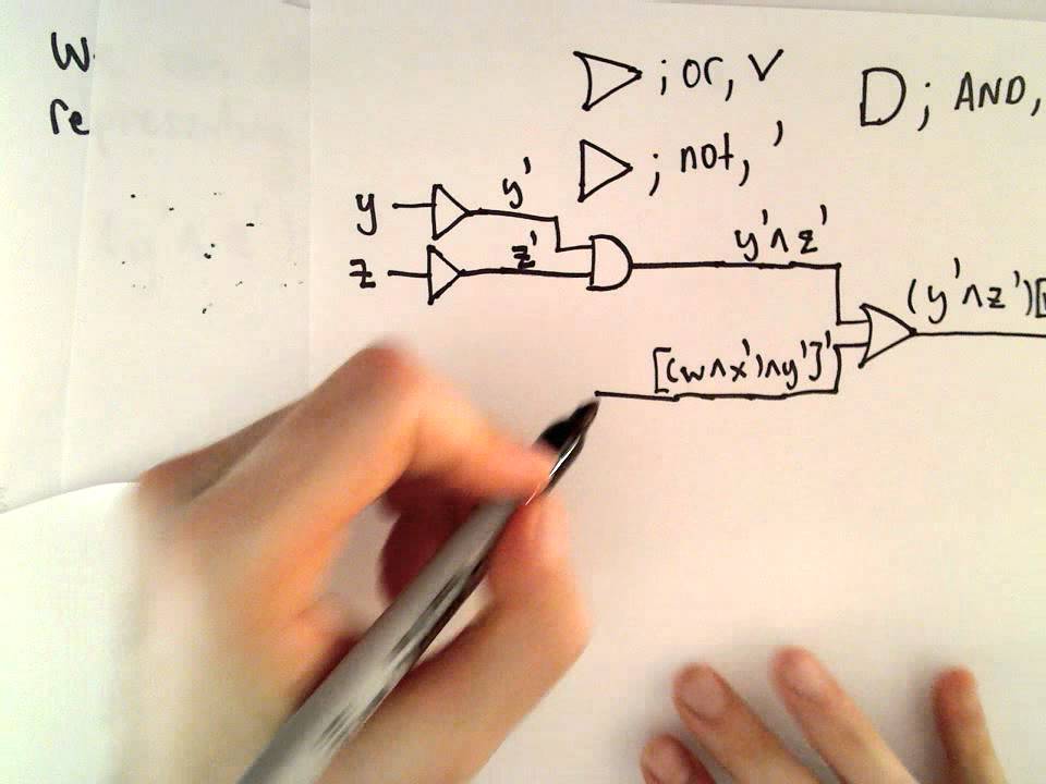
Logical Gates Drawing A Circuit That Corresponds To A Boolean Expression Part 4 Youtube

Demultiplexer An Overview Sciencedirect Topics

Overview Sequential Circuit Design Specification Formulation Ppt Video Online Download