Cvd Graphene Copper Etching

Clean And Efficient Transfer Of Cvd Grown Graphene By Electrochemical Etching Of Metal Substrate Sciencedirect

Cvd Graphene Growth Transfer Ishigami Group Wiki

New Way To Make Cheap Graphene Thermoelectric Materials Material Science Nanotechnology

Chemical Etching Of Copper Foils For Single Layer Graphene Growth By Chemical Vapor Deposition Sciencedirect

Schematic Illustration For The Preparation Of Cvd Graphene Strips Download Scientific Diagram
Cvd Graphene

Synthesis of graphene films on copper foils by chemical vapor deposition.
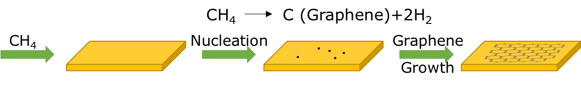
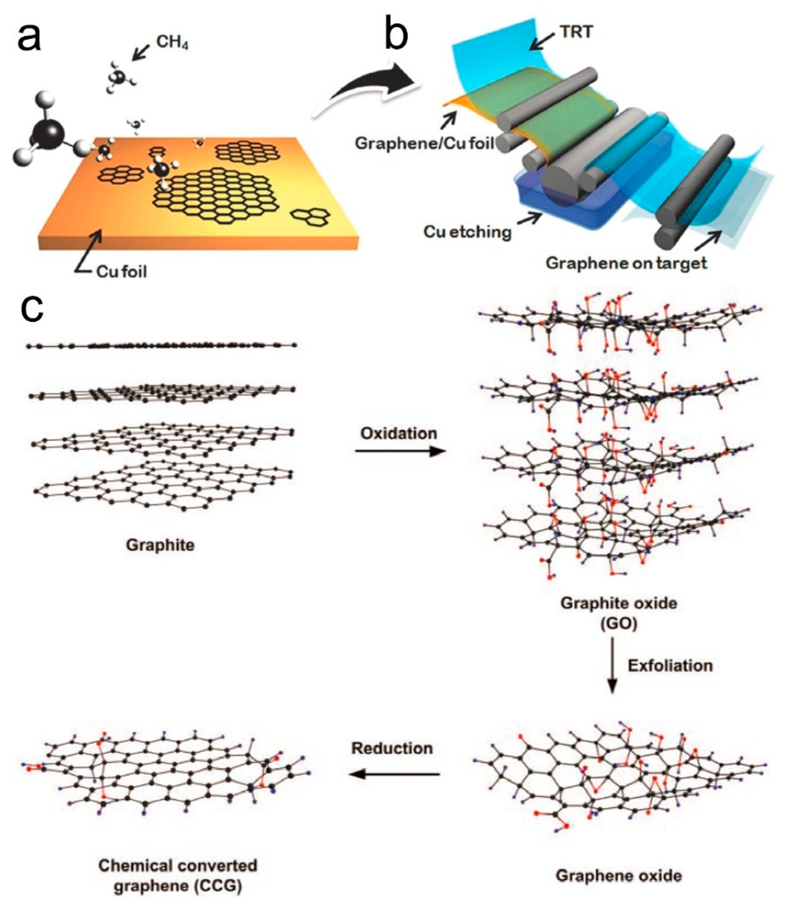
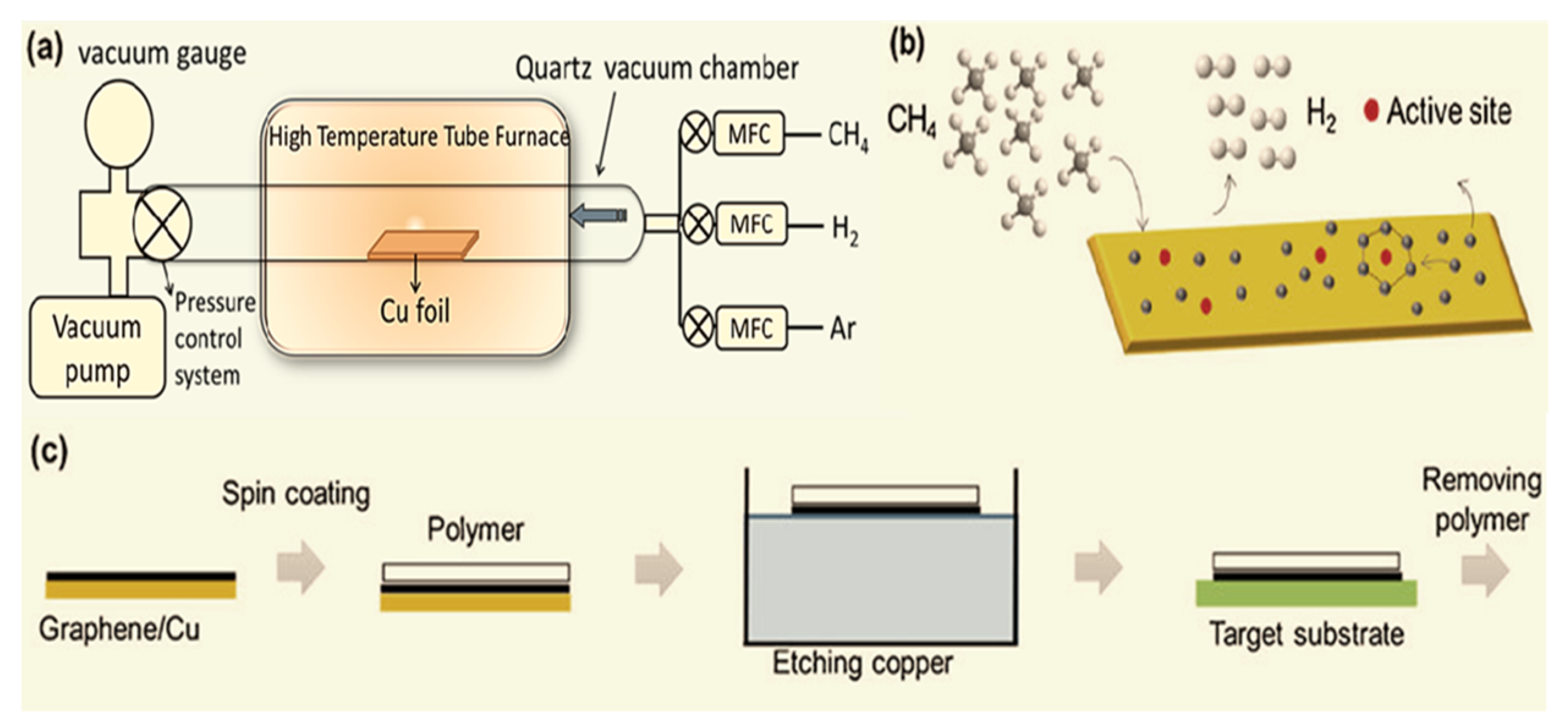
Cvd graphene copper etching. 2a and b show the etching time evolution of the graphene domain size on the copper foils etched by an fecl 3 or an nh 4 2 s 2 o 8 etchant. Graphene grown on copper by chemical vapor deposition cvd has been significantly explored for the synthesis of high quality graphene since the popular recipe for single layer graphene growth was introduced in 2009 1 many years after the first report of the deposition of graphene on cu in 1992 2. We report a simple clean and highly anisotropic hydrogen etching method for chemical vapor deposited cvd graphene catalyzed by the copper substrate. Advanced materials 2016 28 29 6247 6252.
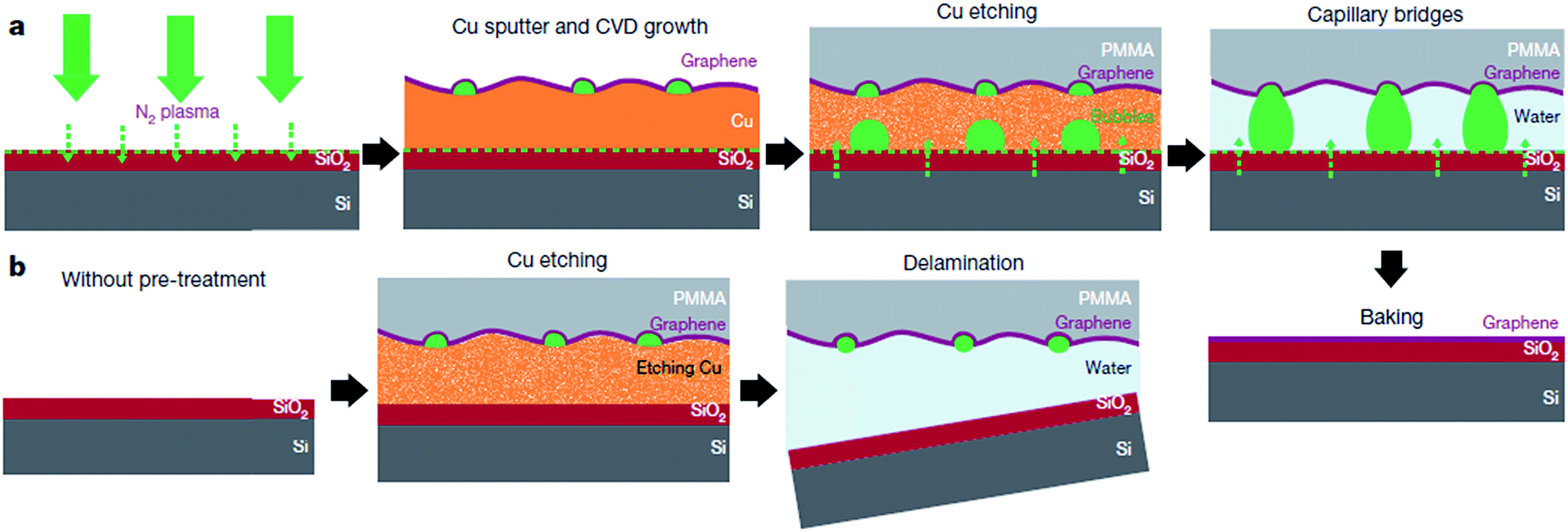
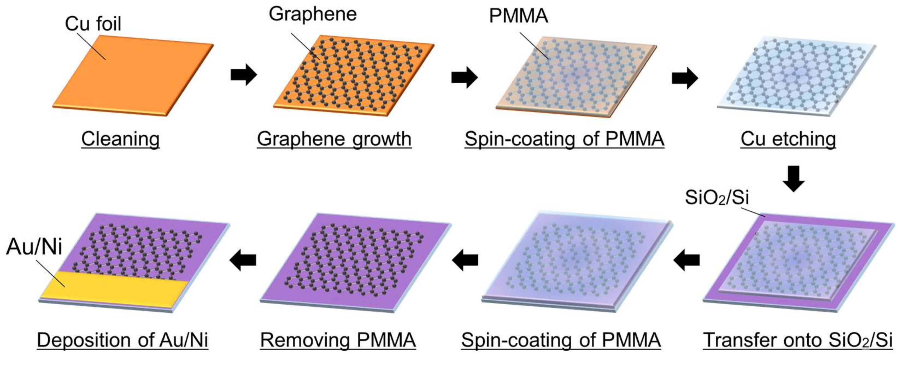
Wei guo feng jing jian xiao ce zhou yuanwei lin shuai wang. After the copper was etched the pmma pva graphene block was rinsed with deionized water three times at 0 c and transferred onto a 100 nm thick sio 2 si substrate. Here to investigate the size and density of the graphene domains the cvd growth of graphene was terminated by stopping the ch 4 feedstock prior to covering the entire cu surface. The pmma pva graphene copper foil block was floated on the surface of a solution of 0 3 m ammonium persulfate aldrich 98 at 0 c for 24 h to etch the copper foil.
Figure 4 shows the raman spectra of the cvd grown bilayer graphene transferred onto pet wafers using the three different etching solutions. In addition we found that the etching is temperature dependent.

Structure And Fabrication Process Of Cvd Grown Graphene On Pet Eva Download Scientific Diagram

Schematics Of The Transfer Process A Chemical Vapor Deposition Cvd Download Scientific Diagram

Monolayer Graphene Transfer Process To Polymeric Substrates A Download Scientific Diagram

Synthesis Based Application Of Graphene Nanotechnology Transistors Touch Screen

Schematic Showing In Situ Etching Process On Cvd Graphene Film For Download Scientific Diagram

Transfer Printing Of A Cvd Grown Graphene Monolayer The Process Download Scientific Diagram

Oil Boundary Approach For Sublimation Enabled Camphor Mediated Graphene Transfer Sciencedirect

Synergistic Oxidation Of Cvd Graphene On Cu By Oxygen Plasma Etching Sciencedirect
Review Of The Synthesis Transfer Characterization And Growth Mechanisms Of Single And Multilayer Graphene Rsc Advances Rsc Publishing Doi 10 1039 C7ra00392g

Direct Observation Of Grain Boundaries In Graphene Through Vapor Hydrofluoric Acid Vhf Exposure Science Advances

Carbon Doped With Nitrogen Dramatically Improves Storage Capacity Of Supercapacitors Thermoelectric Materials Science Nanotechnology

Paraffin Enabled Graphene Transfer Nature Communications

Etching Controlled Growth Of Graphene Fragments On A Cu Surface A Download Scientific Diagram

A Schematic Of Cvd System For Graphene Growth B Schematic Of The Download Scientific Diagram

The Production Of Cu Nanoparticles On Large Area Graphene By Sputtering And In Flight Sintering Unlu 2017 Crystal Research And Technology Wiley Online Library

A I Schematic Process Flow For The Fabrication Of Cvd Graphene Download Scientific Diagram

Direct Transfer Process Of Ultra Large Area Graphene From Cu Foil To Download Scientific Diagram
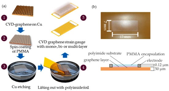
Sensors Free Full Text Strain Gauges Based On Cvd Graphene Layers And Exfoliated Graphene Nanoplatelets With Enhanced Reproducibility And Scalability For Large Quantities Html
Crystals Free Full Text Electrochemical Characterization Of Cvd Grown Graphene For Designing Electrode Biomolecule Interfaces Html

Progress And Challenges In Transfer Of Large Area Graphene Films Chen 2016 Advanced Science Wiley Online Library
Nanomaterials Free Full Text Recent Advances In Graphene Based Humidity Sensors Html
Http Iopscience Iop Org Article 10 1088 2053 1583 Aa69b5 Pdf

Optical Microscopic Image Of Copper Based Cvd Graphene On Sio 2 Si Download Scientific Diagram

The Porosity Of Graphene After Cvd Growth In The Presence Of An Download Scientific Diagram

Neutral Scatterers Dominate Carrier Transport In Cvd Graphene With Ionic Impurities Sciencedirect

Schematic Illustration Of Pva Assisted Transfer Of Cvd Grown 2d Download Scientific Diagram

A Systematic Study Of The Controlled Generation Of Crystalline Iron Oxide Nanoparticles On Graphene Using A Chemical Etching Process Abstract Europe Pmc

Ultrahigh Mobility Graphene Devices From Chemical Vapor Deposition On Reusable Copper Science Advances
Https Www Sciencedirect Com Science Article Am Pii S0008622316307801

Removing Contaminants From Transferred Cvd Graphene Springerlink

A Novel Free Standing Cvd Graphene Platform Electrode Modified With Aupt Hybrid Nanoparticles And L Cysteine For The Selective Determination Of Epinephrine Sciencedirect

Pdf Advances In Transferring Chemical Vapour Deposition Graphene A Review
Single Layer Graphene Membranes By Crack Free Transfer For Gas Mixture Separation Nature Communications

Graphene Based Transparent Conductive Films Material Systems Preparation And Applications Ma 2019 Small Methods Wiley Online Library

Fabrication Of Cgfs A Cu Foil With Graphene Gr On Both Sides Download Scientific Diagram
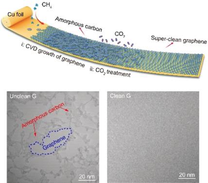
Large Area Synthesis Of Superclean Graphene Via Selective Etching Of Amorphous Carbon With Carbon Dioxide Angew Chem Int Ed X Mol
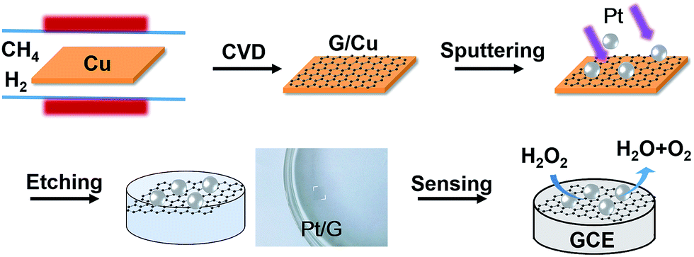
Chemical Vapor Deposition Graphene Combined With Pt Nanoparticles Applied In Non Enzymatic Sensing Of Ultralow Concentrations Of Hydrogen Peroxide Rsc Advances Rsc Publishing Doi 10 1039 C7ra05243j
Mechanical And Electrical Characterization Of Cvd Grown Graphene Transferred On Chalcogenide Ge2sb2te5 Layers Sciencedirect

Schematic Diagram Of The Etching And Scooping Method Without Using A Download Scientific Diagram

Graphene Transfer Process And Afm Imaging A General Graphene Download Scientific Diagram

Transfer Process Of Cvd Graphene To Prepared Sio 2 Nanopillar Download Scientific Diagram

Forschungszentrum Julich Expertise Cvd Graphene
Asi Free Full Text A Brief Description Of Cyclic Voltammetry Transducer Based Non Enzymatic Glucose Biosensor Using Synthesized Graphene Electrodes Html

